Posts

Showing posts from December, 2017

How to Use Analog Comparators in PIC16F877A (Mode-6)
Image
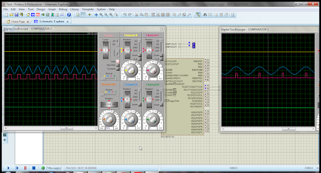
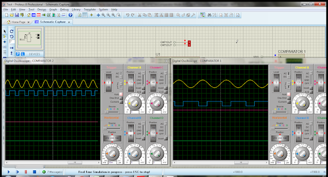
The following code demonstrate how to use analog comparator module in mode-6. In this mode comparator-1 and comparator-2 positive (+) inputs are connected to the comparator voltage reference module. The external inputs are applied on the negative (-) input of comparators. You can map C1OUT and C2OUT on any general purpose IOs. The code is written in “mikroC PRO for PIC v.6.6.3” IDE and simulation is done with Proteus 8.0 SP0. At the end of code, you can find complete project files for download. Code in mikroC // comparator voltage reference formula // when CVRR = 1 // CVREF = (VR<3:0>/24) x (CVRSRC) // Four Inputs Multiplexed to Two Comparators #define CMP_MODE    6 // user assign comparator o/p signals sbit CMP1_Dir at TRISC.B0; sbit CMP2_Dir at TRISC.B1; sbit CMP1_Out at PORTC.B0; sbit CMP2_Out at PORTC.B1; // function proto-type void CMP_Setting(void); void main(void) { CMP1_Dir = 0; CMP2_Dir = 0; // init value CMP1_Out
How to Use Analog Comparators in PIC16F877A (Mode-1)

Image
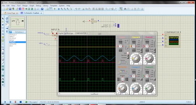
The following code demonstrate how to use analog comparator module in mode-1. In this mode comparator-1 can be used and comparator-2 will be off. The default output of the comparator-1 can be monitor on C1OUT on RA4 pin. You can also map this output on general purpose IOs. The code is written in “mikroC PRO for PIC v.6.6.3” IDE and simulation is done with Proteus 8.0 SP0. At the end of code, you can find complete project files for download. Code in mikroC // One Independent Comparator with Output #define CMP_MODE    1 // default comparators o/p signals sbit C1OUT_Dir at TRISA.B4; sbit C1OUT_Out at PORTA.B4; // user assign comparator o/p signals sbit CMP1_Dir at TRISC.B0; sbit CMP1_Out at PORTC.B0; // function proto-type void CMP_Setting(void); void main(void) { // set direction as output C1OUT_Dir = 0; CMP1_Dir = 0; // init value C1OUT_Out = 0; CMP1_Out = 0; CMP_Setting(); while(1) { C1OUT_Out = CMCON.C1OUT; // user assign

How to Use Analog Comparators in PIC16F877A (Mode-5)

Image
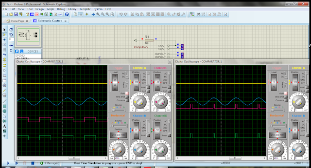
The following code demonstrate how to use analog comparator module in mode-5. In this mode positive input of the two comparators are combine. The default output of each comparator can be monitor on C1OUT on RA4 pin and C2OUT on RA5 pin. You can also map theses outputs on general purpose IOs. The code is written in “mikroC PRO for PIC v.6.6.3” IDE and simulation is done with Proteus 8.0 SP0. At the end of code, you can find complete project files for download. Code in mikroC // Two Common Reference Comparators with Outputs #define CMP_MODE    5 // default comparators o/p signals sbit C1OUT_Dir at TRISA.B4; sbit C2OUT_Dir at TRISA.B5; sbit C1OUT_Out at PORTA.B4; sbit C2OUT_Out at PORTA.B5; // user assign comparator o/p signals sbit CMP1_Dir at TRISC.B0; sbit CMP2_Dir at TRISC.B1; sbit CMP1_Out at PORTC.B0; sbit CMP2_Out at PORTC.B1; // function proto-type void CMP_Setting(void); void main(void) { // set direction as output C1OUT_Dir

How to Use Analog Comparators in PIC16F877A (Mode-4)

Image
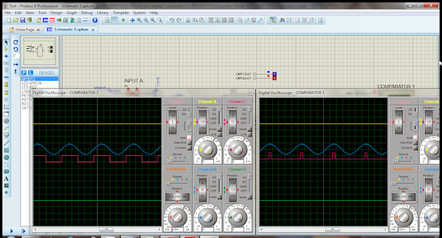
The following code demonstrate how to use analog comparator module in mode-4. In this mode reference is common for two comparators. You can map output-1 C1OUT and output-2 C2OUT on any general purpose IOs. The code is written in “mikroC PRO for PIC v.6.6.3” IDE and simulation is done with Proteus 8.0 SP0. At the end of code, you can find complete project files for download. Code in mikroC // Two Common Reference Comparators #define CMP_MODE    4 // user assign comparator o/p signals sbit CMP1_Dir at TRISC.B0; sbit CMP2_Dir at TRISC.B1; sbit CMP1_Out at PORTC.B0; sbit CMP2_Out at PORTC.B1; // function proto-type void CMP_Setting(void); void main(void) { // set direction as output CMP1_Dir = 0; CMP2_Dir = 0; // init value CMP1_Out = 0; CMP2_Out = 0; CMP_Setting(); while(1) { // user assign comparators o/p signals CMP1_Out = CMCON.C1OUT; CMP2_Out = CMCON.C2OUT; } } void CMP_Setting(void) { //Comparators Reset #i
How to Use Analog Comparators in PIC16F877A (Mode-3)

Image
The following code demonstrate how to use analog comparator module in mode-3. In this mode two independent comparators are used with by default output mapped on C1OUT on RA4 pin and C2OUT on RA5 pin. You also can map theses outputs on general purpose IOs. The code is written in “mikroC PRO for PIC v.6.6.3” IDE and simulation is done with Proteus 8.0 SP0. At the end of code, you can find complete project files for download. Code in mikroC // Two Independent Comparators with Outputs #define CMP_MODE    3 // default comparators o/p signals sbit C1OUT_Dir at TRISA.B4; sbit C2OUT_Dir at TRISA.B5; sbit C1OUT_Out at PORTA.B4; sbit C2OUT_Out at PORTA.B5; // user assign comparator o/p signals sbit CMP1_Dir at TRISC.B0; sbit CMP2_Dir at TRISC.B1; sbit CMP1_Out at PORTC.B0; sbit CMP2_Out at PORTC.B1; // function proto-type void CMP_Setting(void); void main(void) { // set direction as output C1OUT_Dir = 0; C2OUT_Dir = 0; CMP1_Dir = 0; CMP2

How to Use Analog Comparators in PIC16F877A (Mode-2)

Image
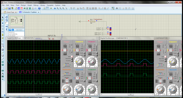
The following code demonstrate how to use analog comparator module in mode-2. In this mode two independent comparators are used and individual comparator output can be maped on any output pin. The code is written in “mikroC PRO for PIC v.6.6.3” IDE and simulation is done with Proteus 8.0 SP0. At the end of code, you can find complete project files for download. Code in mikroC #define CMP_MODE    2 // user assign comparator o/p signals sbit CMP1_Dir at TRISC.B0; sbit CMP2_Dir at TRISC.B1; sbit CMP1_Out at PORTC.B0; sbit CMP2_Out at PORTC.B1; // function proto-type void CMP_Setting(void); void main(void) { // set direction as output CMP1_Dir = 0; CMP2_Dir = 0; // init value CMP1_Out = 0; CMP2_Out = 0; CMP_Setting(); while(1) { // user assign comparators o/p signals CMP1_Out = CMCON.C1OUT; CMP2_Out = CMCON.C2OUT; } } void CMP_Setting(void) { //Comparators Reset #if CMP_MODE == 0 CMCON.CM2 = 0; CMCON.CM1
Basic Understanding of AT89C51

Image
1. Introduction The AT89C51 is a low-power, high-performance CMOS 8-bit microcomputer with 4K bytes of Flash erasable and programmable read only memory (EPROM). It can be erased and program to a maximum of 1000 times. 2. Block Diagram (Resources) The chip has the following available resources: 3. Features The chip has the following features. 4K Bytes of In-System Re-programmable Flash Memory Fully Static Operation: 3 MHz to 24 MHz 128 x 8-bit Internal RAM 32 Programmable I/O Lines Two 16-bit Timer/Counters Five Interrupt Sources Programmable Full Duplex Serial Port Low-power Idle and Power-down Modes 4. Chip Grade and Packages The chip is available in commercial (0° C to 70° C)) and industrial (40° C to 85° C) grade with PDIP (40 pins), PQFP/TQFP (44 pins), and PLCC (44 pins) package. 5. Pin Designation 6. Pin Level Details 6.1. Power Supply Pins VCC Pin 40 provides supply voltage to the chip. The voltage source is +5v GND The pin 20 is des